Analog front-end
Analog measurement. Custom board.
A hashed sample is only as honest as the analog path that produced it. If the front-end clips or the ADC is on the wrong pin, the rest of the stack is decorating a bad number. This page is the board.
The Problem
Digital evidence starts at a physical quantity.
“The sensor said 47 A.” — On which burden, which ADC range, at which Vmid?
“The compressor started.” — Inrush, or a glitch that looked like one?
“We hashed the telemetry.” — After the analog path had already thrown half the sine away.
A transparency log does not rescue a measurement that was wrong at the pin.
The Solution
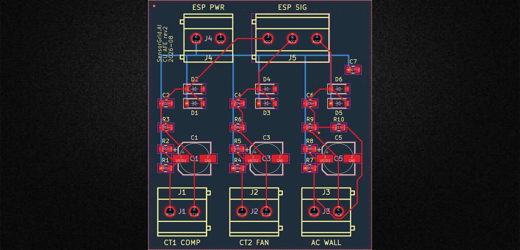
Three-channel analog front-end, generated from a frozen netlist. Two current-transformer inputs and one voltage channel from an AC-AC wall adapter. Clamp-on CTs. Screw terminals. Outputs on P34, P35, and P32 to a separate ESP32.
Netlist as source of truth
The schematic is generated from a frozen netlist. The netlist is the source of truth; the .kicad_sch is not edited by hand.
First article
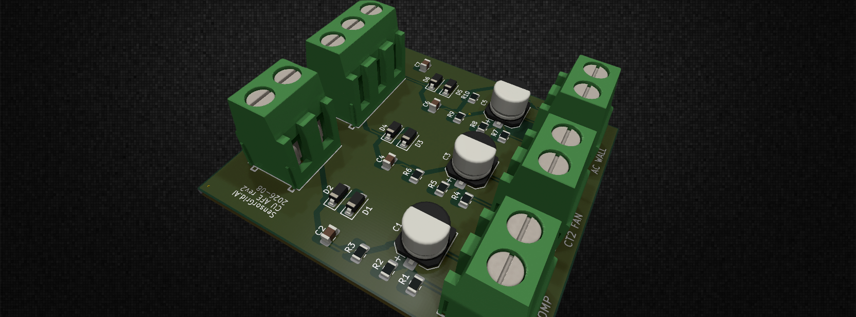
JLCPCB SMT, 2-layer, 46.5 × 52 mm. Resistance of the three bias dividers in parallel: calculated 3.13 kΩ, measured 3.073 kΩ. Six Schottky clamps: 0.204–0.205 V forward, 1 mV spread, orientation confirmed by polarity. Three Vmid nodes: 1.66 V each, half the 3.33 V rail. Voltage channel on 60 Hz: 28.50 V at the adapter, 0.40 V AC at the ADC pin versus ground. The error that would have clipped the sine — lower divider leg to ground instead of Vmid — is ruled out by 1.66 V on that pin with no source attached.
What the first article showed — and what it did not
| Check | Calculated | Measured |
|---|---|---|
| 3V3↔GND (red on 3V3) | 3.13 kΩ | 3.073 kΩ |
| Schottky forward drop ×6 | 0.15–0.35 V | 0.204–0.205 V |
| Upper voltage-divider leg | 68 kΩ | 67.3 kΩ |
| Vmid 1 / 2 / 3 | 1.665 V | 1.66 / 1.66 / 1.66 |
| AC-AC adapter output | 28.6 V | 28.50 V |
| ADC pin, 60 Hz, vs GND | ~0.41 V AC | 0.40 V AC |
Figures in the table are from the project’s first-article log, 6–7 August 2026. What that log records: the three bias dividers in the right ballpark, six clamps conducting the right way, three Vmid nodes at half-rail, the lower divider leg on Vmid not ground, and 60 Hz from the adapter at the ADC pin. That is not a full netlist-to-board proof, not waveform fidelity, not phase, and not metering accuracy.
Not shown on the bench, and not claimed: current-channel accuracy on AC (needs firmware and a calibrated load), and anything about the machine the clamps later went on. Calibration is empirical. A solder-guide model of Vmid impedance did not survive the 60 Hz measurement — rail bounce is percents, not a quarter — and that disagreement is left open.
Technical Foundation
- AFE: two current-transformer channels + a voltage channel from an AC-AC wall adapter. Bias to mid-rail, Schottky clamp, RC at the ADC pin.
- MCU interconnect: P34, P35, P32 to a separate ESP32.
- CAD: KiCad 10. Netlist → generated schematic → board.
- Fab: 2-layer SMT, factory assembled. First article checked against the table above.
Need the analog path owned along with the firmware? Contract engagements cover schematic to first-article acceptance.